LoRa Network Planning and RF Site Surveys: A Practical Engineering Guide
LoRa Network Planning and RF Site Surveys: A Practical Engineering Guide Deploying a LoRa network is far more than selecting a gateway and scattering sensors across a site. Behind every reliable, low-power wide-area network (LPWAN) deployment is a rigorous engineering process—one that starts long before a single packet is transmitted. RF site surveys, propagation modeling,

Aluminum Busbars in California | Local Supply & Custom Orders
Aluminum Busbars in California | Local Supply & Custom Orders
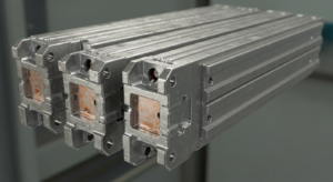
Aluminum Busbars – Electrical Power Solutions
Aluminum busbars serve as a crucial component in lightweight, efficient power distribution systems. These bus bars facilitate the conduction of electrical current, allowing for streamlined electrical power distribution across various applications. Aluminum’s natural lightweight composition makes it an ideal choice for busbars, especially in settings where reducing overall weight is critical, such as in overhead
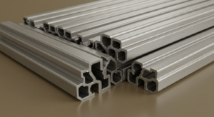
High-Quality Aluminum Busbars for Reliable Power Distribution
High-Quality Aluminum Busbars for Reliable Power Distribution are integral components within power distribution systems, designed to efficiently conduct electricity across different points. A busbar, typically made from aluminum or aluminum alloys, acts as a central hub in electrical systems, ensuring the reliable transmission of power while minimizing energy losses. The choice of aluminum for these

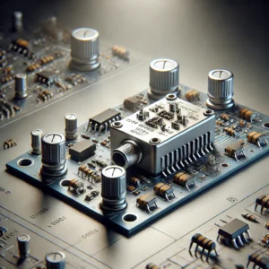
Design of Radio Low Noise Amplifiers (LNAs)
Introduction to LNAs A Low Noise Amplifier (LNA) is an electronic amplifier designed to boost very weak RF signals while adding as little additional noise as possible (Low-noise amplifier – Wikipedia). In a receiver chain, the LNA is typically the first active component after the antenna ( FAQ | ShareTechnote). Its primary role is to
